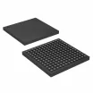
Ball Grid Array Package
Ceramic Ball Grid Array Package becames the best choice for high-density, high-performance, multi-pin packages such as CPUs and south/north bridge chips on motherboards.Please contact us if you are interested.
Product Description
In the 1990s, with the advancement of integration technology, the improvement of equipment, and the use of deep submicron technology, LSI, VLSI, and ULSI appeared one after another. The integration level of silicon single chips continued to increase, and the requirements for integrated circuit packaging became stricter. With a sharp increase, the power consumption also increases. In order to meet the needs of development, on the basis of the original packaging varieties, a new variety has been added - ball grid array packaging, referred to as BGA (Ball Grid Array Package).
Basic Information
Name: Ball Grid Array Package
Abbreviation: BGA
Features: The thickness is reduced by more than 1/2 compared with QFP, etc.
Classification: PBGA substrate, CBGA substrate
Ball Grid Array Technology Introduction
The memory packaged with BGA technology can increase the memory capacity by two to three times while maintaining the same volume. Compared with TSOP, BGA has smaller volume, better heat dissipation performance and electrical performance. BGA packaging technology has greatly improved the storage capacity per square inch. Under the same capacity, memory products using BGA packaging technology are only one-third of the volume of TSOP packaging; in addition, compared with traditional TSOP packaging methods, BGA packaging There is a faster and more effective way to dissipate heat.
The I/O terminals of the BGA package are distributed under the package in the form of circular or columnar solder joints in an array. The advantage of BGA technology is that although the number of I/O pins has increased, the pin spacing has not decreased but increased, thus The assembly yield is improved; although its power consumption increases, BGA can be welded with a controlled collapse chip method, which can improve its electrothermal performance; the thickness and weight are reduced compared with previous packaging technologies; parasitic parameters (large current When the amplitude changes, the output voltage disturbance) decreases, the signal transmission delay is small, and the frequency of use is greatly increased; the assembly can be coplanar welding, and the reliability is high.
With its global supply network and years of market experience, Oude Electronics can provide the most accurate spot information, including manufacturer, material code, production date, price, ROHS standard, packaging information and arrival date.
Ball Grid Array Package Features
As soon as BGA appeared, it became the best choice for high-density, high-performance, multi-functional and high I/O pin packaging of VLSI chips such as CPUs and North-South Bridges. Its characteristics are:
1. Although the number of I/O pins has increased, the pin spacing is much larger than that of QFP, which improves the assembly yield;
2. Although its power consumption increases, BGA can be soldered by the controlled collapse chip method, referred to as C4 soldering, which can improve its electrothermal performance;
3. The thickness is reduced by more than 1/2 than that of QFP, and the weight is reduced by more than 3/4;
4. The parasitic parameters are reduced, the signal transmission delay is small, and the frequency of use is greatly increased;
5. Coplanar welding can be used for assembly, with high reliability;
6. BGA packaging is still the same as QFP and PGA, occupying too much substrate area;
Intel Corporation uses ceramic needle grid array package CPGA and ceramic ball grid array package for this kind of CPU chip with high integration (more than 3 million transistors in a single chip) and high power consumption, such as Pentium, Pentium Pro, and Pentium II. CBGA, and install a miniature exhaust fan on the shell to dissipate heat, so as to achieve stable and reliable operation of the circuit.
BGA ball grid array package
With the development of integrated circuit technology, the packaging requirements for integrated circuits are more stringent. This is because the packaging technology is related to the functionality of the product. When the frequency of the IC exceeds 100MHz, the traditional packaging method may produce the so-called "CrossTalk" phenomenon, and when the number of pins of the IC is greater than 208 Pins, the traditional packaging method has its difficulty. Therefore, in addition to using the QFP packaging method, most of today's high-pin-count chips (such as graphics chips and chipsets, etc.) have turned to BGA (Ball Grid Array Package) packaging technology. As soon as BGA appeared, it became the best choice for high-density, high-performance, multi-pin packages such as CPUs and south/north bridge chips on motherboards.
Key Features:
♦Advanced Packaging Technology: The BGA Package utilizes an organic substrate, which is cost-effective and widely used in modern electronics manufacturing. It is designed to accommodate a large number of solder balls that provide a high-density interconnect solution, making it ideal for high-performance applications.
♦Reliable Solder Balls: The BGA Package features high-quality solder balls, which are available in both leaded and lead-free options, making it compliant with environmental regulations. These solder balls ensure reliable electrical connections and are designed to withstand the stresses of thermal cycling and mechanical shock.
♦Efficient Heat Dissipation: The BGA Package is designed with a large thermal pad on the bottom of the package, which enables efficient heat dissipation. This feature is crucial for high-performance applications where heat management is critical to ensure optimal device performance and reliability.
♦Easy Assembly: The BGA Package is designed for ease of assembly, making it suitable for high-volume production. The solder balls are arranged in a regular grid pattern, allowing for automated assembly using pick-and-place machines. This reduces assembly time and labor costs, making it a cost-effective solution for electronic manufacturers.
Classification
1. PBGA (Plastic BGA) substrate: generally a multilayer board composed of 2-4 layers of organic materials. Among Intel series CPUs, Pentium II, III, and IV processors all use this package. In the past two years, another form has appeared: that is, the IC is directly bonded to the board. Its price is much cheaper than the regular price, and it is generally used in games and other fields that do not have strict quality requirements.
2. CBGA (CeramicBGA) substrate: that is, a ceramic substrate, and the electrical connection between the chip and the substrate is usually installed by flip chip (FlipChip, FC for short). Among Intel series CPUs, Pentium I, II, and Pentium Pro processors have all used this package.
3. FCBGA (FilpChipBGA) substrate: hard multi-layer substrate.
4. TBGA (TapeBGA) substrate: The substrate is a strip-shaped soft 1-2 layer PCB circuit board.
5. CDPBGA (Carity Down PBGA) substrate: refers to the chip area (also known as the cavity area) with a square depression in the center of the package.
Differences Between CBGA (Ceramic Ball Grid Array) and BGA (Ball Grid Array):
| Feature | CBGA | BGA |
|---|---|---|
| Material | Ceramic substrate | Organic substrate |
| Solder Balls | Leaded or lead-free | Leaded or lead-free |
| Package Size | Typically larger | Can be smaller |
| Heat Dissipation | Good heat dissipation | Moderate heat dissipation |
| Reliability | Higher reliability | Lower reliability |
| Cost | Typically more expensive | Typically less expensive |
| Electrical Performance | Better electrical performance | Good electrical performance |
| Applications | High-performance applications | General applications |
| Assembly | Requires higher level of expertise | Easier to assemble |
Note: CBGA is less commonly used nowadays due to concerns about lead content in electronics. BGA has become more popular with the widespread adoption of lead-free soldering in electronics manufacturing.
Applications of BGA ball grid array:
♦Microprocessors
♦Graphics processing units (GPUs)
♦Application-specific integrated circuits (ASICs)
♦High-speed communication devices
♦Aerospace and defense systems
♦Automotive electronics
♦Industrial control systems
Electronic Parts Supply
| BGA |
| MCF5282CVM66 |
| SAK-TC297TP-128F300N BC |
| MK70FN1M0VMJ12 |
| MT29F2G08ABAEAH4:E |
| MT25QL128ABA8E12-0SIT |
| IS42S16160G-7BLI-TR |
| MT29F4G08ABBDAH4:D |
| MT41K128M16JT-125:K |
| MT41K256M16TW-107:P |
| MT47H64M16NF-25E:M |
| MT29F2G08ABAEAH4-IT:E |
| M24C64-FCS6TP/K |
| XC7K325T-2FFG900I |
| XC7K325T-2FFG676I |
| XC5VSX95T-1FFG1136I |
| XC7K325T-2FFG676I |
| XC7K160T-2FFG676I |
| XC7K410T-2FFG900I |
| XC7Z100-2FFG900I |
| XC5VLX110T-1FFG1136I |
| XC5VSX50T-1FFG665I |
| XC5VLX155T-1FFG1136I |
| XC5VSX95T-2FFG1136I |
| SAK-TC399XX-256F300S BD |
| SAK-TC377TP-96F300S AA |
| SAK-TC387QP-160F300S AE |
| SAK-TC397XP-256F300S BD |
| MCIMX6X4AVM08AB |
| MCIMX515DJM8C |
| MCIMX6U6AVM08AC |
| MCIMX6Q6AVT10AD |
| MCIMX6D6AVT10AD |
| MCIMX6Q5EYM10AD |
| AT91SAM9260B-CU |
| TMS320C5505AZCH15 |
| ADSP-BF512BBCZ-4 |
| TPS63806YFFR |
| LMR70503TMX/NOPB |
| TPS62180YZFR |
| MT28EW256ABA1HPC-0SIT |
| MT28EW256ABA1HPC-0SIT |
| XC6SLX9-2CSG225I |
| XC6SLX9-2FTG256C |
| XC6SLX9-2TQG144I |
| XC6SLX16-2FTG256C |
| XC6SLX16-2CSG324C |
| XC6SLX16-2CSG324I |
| XC6SLX25-2FTG256C |
| XC7S75-1FGGA484C |
Reliable Electronic Components Supplier-Oude Electronics
Oude BGA Package offers advanced electronic packaging technology that delivers superior performance, reliability, and ease of assembly. With its efficient heat dissipation, high-density interconnects, and reliable solder balls, it is an ideal choice for high-performance electronic applications. Contact us to learn more about how our BGA Package can meet the unique needs of your electronic products.
FAQ about Ball Grid Array Package
1.Q: What is a Ball Grid Array (BGA) Package?
A: BGA Package is an advanced electronic packaging technology that utilizes an organic substrate and solder balls to provide reliable electrical connections for high-performance electronic devices.
2.Q: How does a BGA Package work?
A: BGA Package consists of an organic substrate with an array of solder balls on the bottom surface. These solder balls serve as the electrical contacts that connect the package to the printed circuit board (PCB) or other electronic components. The BGA Package is typically mounted on the PCB using soldering techniques, and the solder balls form the interconnects for electrical signals and power.
3.Q: What are the advantages of using a BGA Package?
A:The advantages of using a BGA Package include:
•High-density interconnects: BGA Package allows for a large number of solder balls in a regular grid pattern, providing a high-density interconnect solution, ideal for high-performance applications.
•Efficient heat dissipation: BGA Package is designed with a large thermal pad on the bottom, enabling efficient heat dissipation, crucial for managing heat in high-performance electronic devices.
•Reliable electrical connections: The solder balls in BGA Package provide reliable electrical connections, ensuring high-quality signal transmission and power delivery.
•Ease of assembly: BGA Package is designed for automated assembly, reducing assembly time and labor costs in high-volume production.
4.Q: What are the typical applications of BGA Package?
A: BGA Package is commonly used in a wide range of high-performance electronic applications, including microprocessors, GPUs, ASICs, high-speed communication devices, aerospace and defense systems, automotive electronics, and industrial control systems.
5.Q: Can BGA Packages be used in lead-free applications?
A: Yes, BGA Packages are available in both leaded and lead-free options, making them compliant with environmental regulations such as RoHS (Restriction of Hazardous Substances) directive.
6.Q: Are there any challenges in using BGA Packages?
A: While BGA Packages offer many advantages, there are some challenges associated with them, such as the need for careful design considerations to ensure proper heat dissipation, the requirement for advanced assembly techniques, and the need for thorough inspection and testing due to the hidden nature of solder joints.
7.Q: How reliable are BGA Packages?
A: BGA Packages are designed to be highly reliable when properly designed, assembled, and tested. However, like any electronic component, they can be subject to failure due to various factors such as mechanical stress, thermal cycling, and environmental conditions. Proper design, manufacturing, and testing processes are important to ensure the reliability of BGA Packages in electronic devices.
8.Q: Can BGA Packages be repaired or reworked?
A: Repairing or reworking BGA Packages can be challenging due to the hidden nature of solder joints. It requires specialized tools and expertise to remove and replace a BGA Package without causing damage to the PCB or the package itself. However, in some cases, BGA Packages can be repaired or reworked by skilled technicians using appropriate techniques and equipment.
9.Q: How can I choose the right BGA Package for my application?
A: Choosing the right BGA Package for your application requires careful consideration of factors such as electrical requirements, thermal management needs, assembly capabilities, reliability requirements, and cost constraints. Consulting with experienced engineers or contacting BGA Package manufacturers for technical support can help in selecting the appropriate BGA Package for your specific application.


