Quad Flat No-leads Package
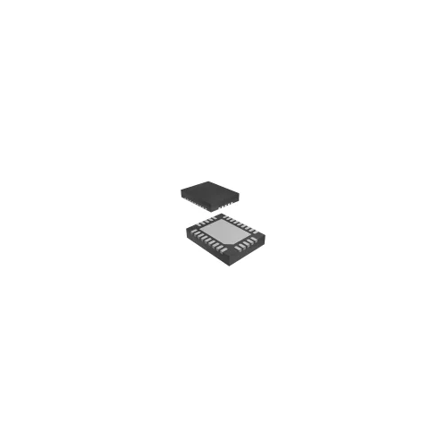
QFN packages(Quad Flat No-leads Package / Quad Flat No Leads Package) come in a variety of sizes and configurations, including versions with exposed pads on the bottom of the package for improved thermal performance. They are commonly used in mobile devices, consumer electronics, and other small form factor applications.
Product Description
QFN packages(Quad Flat No-leads Package / Quad Flat No Leads Package) come in a variety of sizes and configurations, including versions with exposed pads on the bottom of the package for improved thermal performance. They are commonly used in mobile devices, consumer electronics, and other small form factor applications.
QFN (Quad Flat No-leads Package,Quad Flat No Leads Package), one of the surface mount packages. It is worth noting that the QFN package is completely different from the LCC package. The LCC still has extension pins, but the pins are bent to the bottom, while the QFN package does not have any extension pins at all. QFN is a name stipulated by the Japan Electron Machinery Industry Association.
Quad Flat No Leads (QFN) package is a type of surface mount technology package used for integrated circuits (ICs). It is a variation of the Quad Flat Package (QFP) with the leads extending out from the sides of the package instead of from the bottom.
QFN packages have a flat square or rectangular body with a lead frame on the perimeter of the package. The lead frame is either an etched pattern on the surface of the package or a metal frame that is stamped or etched and then attached to the package. The leads are usually arranged in a grid pattern and are very small, making QFNs suitable for small form factor applications.
The advantage of the QFN package is that it provides a small, low profile package with good thermal and electrical performance. Leadless Package with a Rectangular Shape also allows for easy automated assembly using surface mount technology. The lack of leads on the bottom of the package also means that there is more space on the PCB for other components or routing.
Rectangular Shape Leadless Package comes in a variety of sizes and configurations, including versions with exposed pads on the bottom of the package for improved thermal performance. They are commonly used in mobile devices, consumer electronics, and other small form factor applications.

Our Partner
Oude was formerly a distributor of electronic components in Mainland China, and has developed in the Mainland for 20 years!At present, we serve OEM, ODM, EMS, CM, and the fields involved include consumer electronics, medical equipment, automobiles, industrial automation, aerospace military and other fields!Get In Touch With Us Instantly!
Basic Information
Name: Quad Flat No-leads Package / Quad Flat No Leads Package
Abbreviation: QFN
Nature: One of the surface mount packages
Introduction
QFN (Quad Flat No-leads Package, Quad Flat No-leads Package), one of the surface mount packages. QFN is a name specified by the Japan Electron Machinery Industry Association. There are electrode contacts on the four sides of the package. Since there are no leads, the mounting area is smaller than that of QFP, and the height is lower than that of QFP. However, when stress occurs between the printed substrate and the package, it cannot be relieved at the electrode contact. Therefore, it is difficult to have as many electrode contacts as there are QFP pins, generally from 14 to 100. The materials are ceramic and plastic. Basically ceramic QFN when there is LCC mark. The electrode contact center distance is 1.27mm. Plastic QFNs are a low-cost package on a glass epoxy printed substrate substrate. In addition to 1.27mm, the electrode contact center distance also has two types: 0.65mm and 0.5mm. This package is also known as plastic LCC, PCLC, P-LCC, etc.
QFN Package Types and QFN Package Sizes
| Package Type | Package Size (mm) | Pins | Exposed Pad Size (mm) |
|---|---|---|---|
| QFN-16 | 3 x 3 | 16 | 1.5 |
| QFN-20 | 3.5 x 3.5 | 20 | 2.0 |
| QFN-24 | 4 x 4 | 24 | 2.5 |
| QFN-28 | 5 x 5 | 28 | 3.0 |
| QFN-32 | 5 x 5 | 32 | 4.0 |
| QFN-40 | 6 x 6 | 40 | 4.0 |
| QFN-48 | 7 x 7 | 48 | 5.0 |
| QFN-64 | 9 x 9 | 64 | 6.0 |
| QFN-80 | 10 x 10 | 80 | 7.0 |
| QFN-100 | 12 x 12 | 100 | 8.0 |
Note that the package sizes and pin counts may vary depending on the manufacturer and specific application requirements. The exposed pad size is also an important consideration for thermal management and may vary depending on the power dissipation of the IC.
Leadless Package with a Rectangular Shape Features
QFN is a leadless package with a square or rectangular shape. There is a large-area exposed pad at the center of the bottom of the package for heat conduction, and there are conductive pads around the periphery of the package around the large pad for electrical connection. Because the QFN package does not have gull-wing leads like the traditional SOIC and TSOP packages, the conductive path between the internal pins and the pad is short, the self-inductance coefficient and the internal wiring resistance of the package are very low, so it can provide excellent electrical performance. In addition, it provides excellent thermal performance through the exposed lead frame pad, which has a direct thermal channel to dissipate heat inside the package. Thermal pads are usually soldered directly to the board, and thermal vias in the PCB help spread excess power dissipation into the copper ground plane, which absorbs excess heat.
►Small form factor package suitable for small electronic devices
►Low profile design for space-constrained applications
►Leadless bottom design provides more space on the PCB for other components or routing
►Good thermal and electrical performance due to its design
►Easy automated assembly using surface mount technology
►Variety of sizes and configurations to choose from
The pad design of QFN mainly has three aspects: ① pad design of peripheral pins; ② design of intermediate thermal pad and via hole; ③ consideration of PCB solder mask structure.
Advantages of Leadless Package with a Rectangular Shape:
①QFN packages offer a low profile design, making them suitable for space-constrained applications
②The leadless bottom design provides more space on the PCB for other components or routing, allowing for greater flexibility in design
③The good thermal and electrical performance of QFNs ensures reliable operation
④Easy automated assembly using surface mount technology reduces the manufacturing cost and time
Rectangular Shape Leadless Package Applications:
►Mobile devices
►Consumer electronics
►Industrial automation
►Aerospace and defense
►Automotive electronics
►Medical devices
Some Common Problems with Electronic Components
Electronic Components Datasheet
| QFN |
| TPS53513RVER |
| LT8614EUDC#TRPBF |
| KSZ8041NLI-TR |
| KSZ8721BL-TR |
| LT8614EUDC#TRPBF |
| LT8610EMSE#TRPBF |
| TPS650250RHBR |
| TPS51200DRCR |
| TPS54620RGYR |
| TPS51200DRCR |
| TRS3253EIRSMR |
| MSP430FR2433IRGER |
| TPS62130ARGTR |
| TPS53353DQPR |
| TPS53319DQPR |
| USB2422/MJ |
| KSZ8851SNL-TR |
| LAN9500A-ABZJ-TR |
| KSZ8794CNXCC-TR |
| STM32L011F4U6TR |
| STM32G031G8U6 |
| STM32L412CBU6 |
| STM32L432KBU6 |
| STM32L431CCU6 |
| STM32L451CEU6 |
| MSP430F2272IRHAR |
| MSP430FR2673TRHBR |
| PIC18F25K83-I/ML |
| ATMEGA32U2-MU |
| PIC32MX250F128B-I/ML |
| DSPIC33FJ64GP802-I/MM |
| PIC24FJ256GA106-I/MR |
| PIC18LF2580-I/ML |
| ATTINY1634-MUR |
| ATTINY85-20MU |
| PIC18F26K83-E/ML |
| ATMEGA32U4RC-MUR |
| DSPIC33FJ64MC802-I/MM |
| ATSAM4LS8BA-MU |
| ATTINY88-MMU |
| ATTINY44A-MUR |
| PIC18F46J50T-I/ML |
| MSP430G2855IRHA40T |
| MSP430F2132IRHBT |
| MSP430F2370IRHAT |
| MSP430F5500IRGZT |
| MSP430F5171IRSBT |
| MSP430F249TRGCR |
| MSP430F2013IRSAR |
Integrated Circuit Package Types
1.Dual In-Line Package (DIP): A DIP package has two rows of pins extending from the bottom of the package. The pins are spaced apart at a standard 0.1 inch (2.54 mm) pitch. DIP packages are commonly used for through-hole mounting on a printed circuit board (PCB).
2.Small Outline Integrated Circuit (SOIC): An SOIC package has leads that extend from two opposite sides of the package. The leads are spaced at a standard 0.05 inch (1.27 mm) pitch, making SOIC packages suitable for high-density mounting on a PCB.
3.Quad Flat Package (QFP): A QFP package has leads that extend from all four sides of the package. The leads are arranged in a grid pattern and are very small, making QFPs suitable for small form factor applications.
4.Ball Grid Array (BGA): A BGA package has an array of solder balls on the bottom of the package. The solder balls provide electrical connections between the package and the PCB. BGAs are commonly used for high-performance applications, as they provide excellent thermal and electrical performance.
5.Quad Flat No-Leads (QFN): A QFN package is similar to a QFP package, but the leads extend out from the sides of the package instead of from the bottom. QFN packages are low profile and provide good thermal and electrical performance, making them suitable for small form factor applications.
These are just a few examples of the many types of IC packages available. The main differences in connection between these packages lie in the number of pins, the pitch of the pins, and the location of the pins on the package. These factors determine how the package is mounted on the PCB and how it is connected to other components in the circuit.
The latest innovation in IC package types - the Quad Flat No-leads Package (QFN). This leadless package boasts a rectangular shape, making it an ideal choice for compact and space-constrained applications. With its streamlined design and absence of leads, QFN packages offer improved electrical performance and reduced signal interference.
The rectangular shape leadless package of the QFN is designed to minimize the footprint of the IC, allowing it to be mounted on a PCB with greater density and efficiency. The lack of leads also simplifies the manufacturing process, reducing the risk of defects and improving reliability.
QFN packages come in a range of sizes and pin counts, making them suitable for a wide range of applications, from mobile devices and consumer electronics to automotive and industrial equipment. Additionally, the exposed pad on the underside of the package serves as a thermal pad, providing effective heat dissipation for high-performance ICs.
Upgrade your design with the QFN package, the latest innovation in IC packaging technology. Experience improved electrical performance, simplified manufacturing, and compact design with this leadless package featuring a rectangular shape.
